Expanding the possibilities of cutting-edge 5G/IoT electronic devices and on-board sensors through high-precision,
Expanding the possibilities of cutting-edge 5G/IoT electronic devices and on-board sensors through high-precision,
Consult with us from the planning stage of new development!Overseas transactions amount to over 50%.We can offer direct sales to overseas customers.
Accelerating the evolution of electronic devices along with IoT and 5G industries
Accelerating the evolution of electronic devices along with the IoT and 5G industries
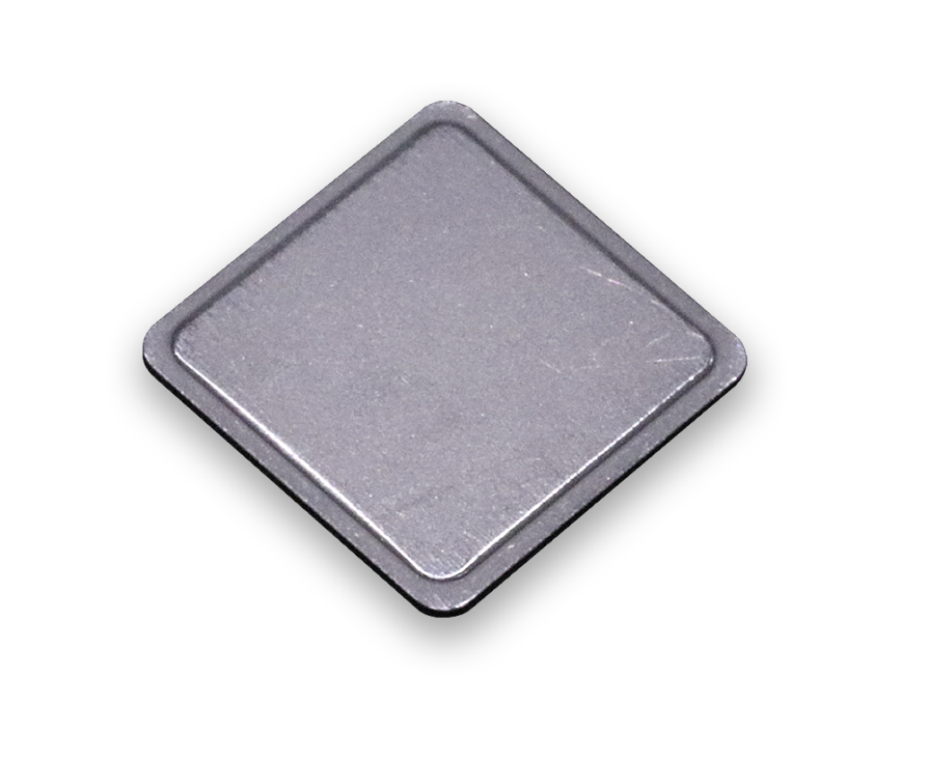
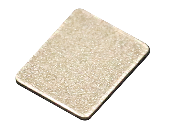
A history and track record of producing lids and caps, which are indispensable for ceramic packages.
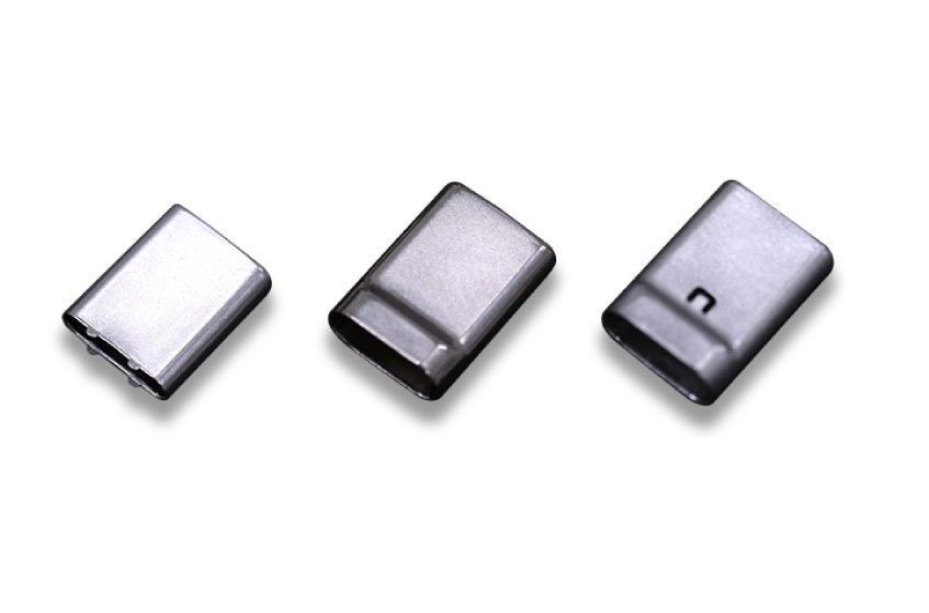
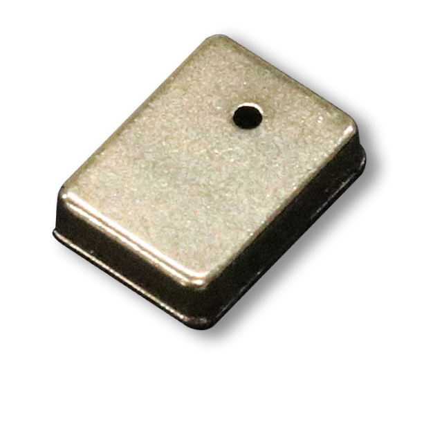
 Lid (left) and stepped lid (right) for crystal devices
Constant advances are being made in the field of electronic
devices.
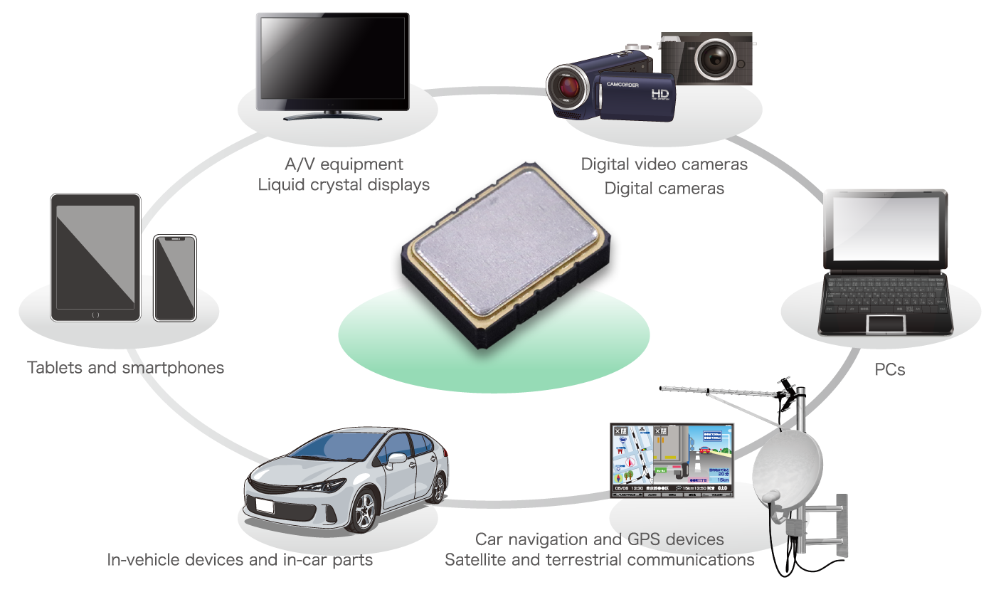
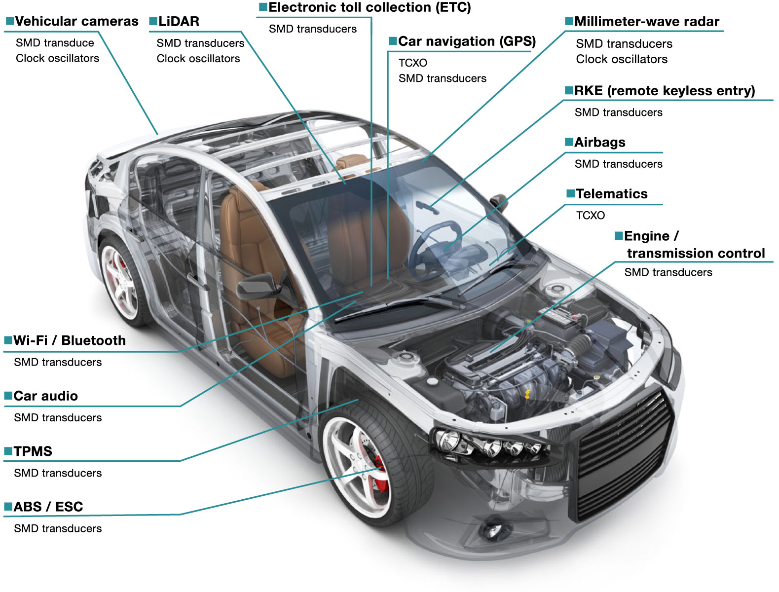
Crystal devices have immeasurable potential, as their usage is
expanding to include in-vehicle devices such as self-driving
systems and advanced driver-assistance systems (ADAS).
We are proud of our history and track record in high-precision
press machining technology for products such as lids and caps,
which are indispensable for crystal devices.
YHPC’s metalworking technology is also useful for LiDAR cases, which are essential for self-driving vehicles.
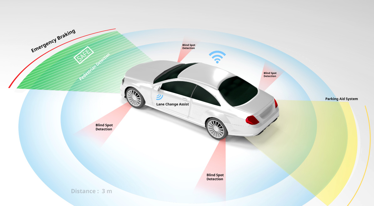 Illustration of how self-driving sensing works
LiDAR* is a technology for instantly and accurately sensing people, objects, and other obstacles in the vehicle’s vicinity, using light sensors for detection and distance measurement. It is one of the key safety components of ADAS (advanced driver-assistance systems), which will soon be mainstream and are indispensable for increasingly widespread self-driving vehicles. At Yoshikawa Hi-Precision Kimitsu Factory, we are also developing technology for bonding pressed metal case parts for LiDAR receivers to glass. Sensors are protected by applying high-accuracy precision machining technology during driving in outdoor environments with extreme temperature changes and the effects of vibration. Safe, secure driving is achieved through reliable sensing.
*An acronym for light detection and ranging


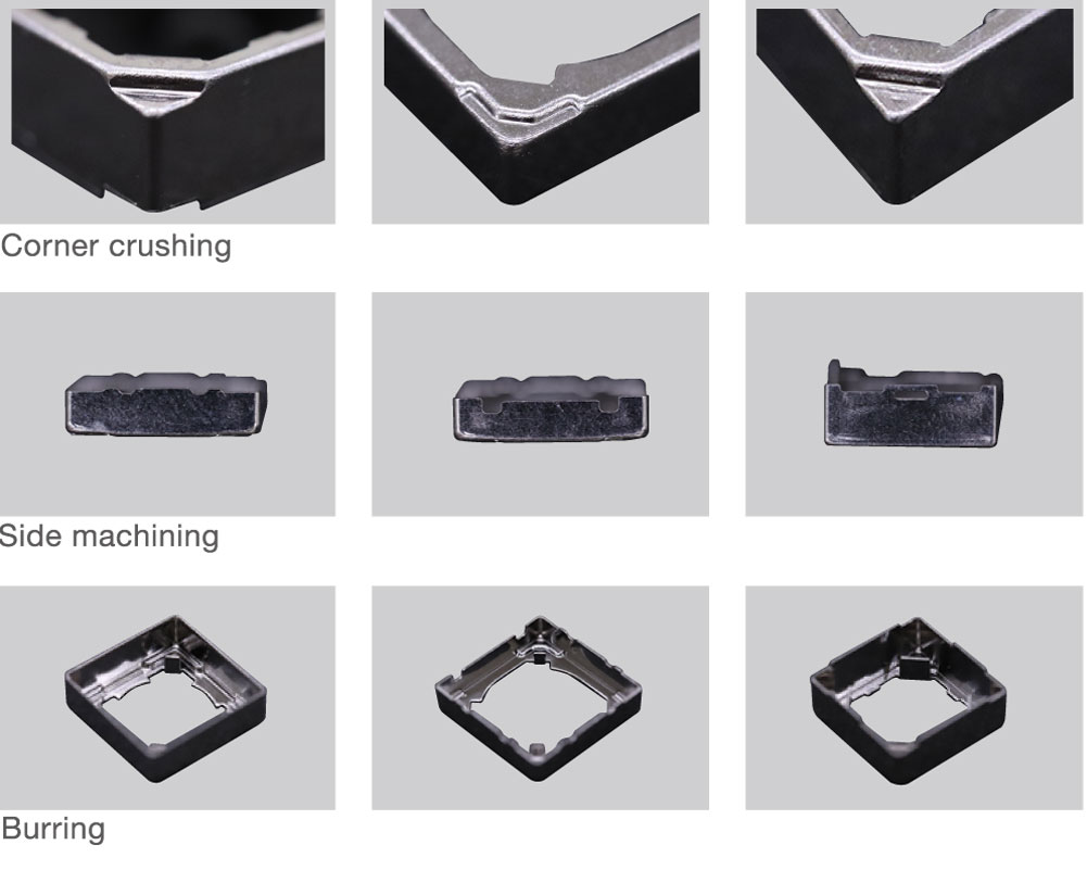
We’ve achieved the world’s first non-etched press-manufactured stepped lids.

Monthly volumes of 600 million units!
Nine keywords related to lid production
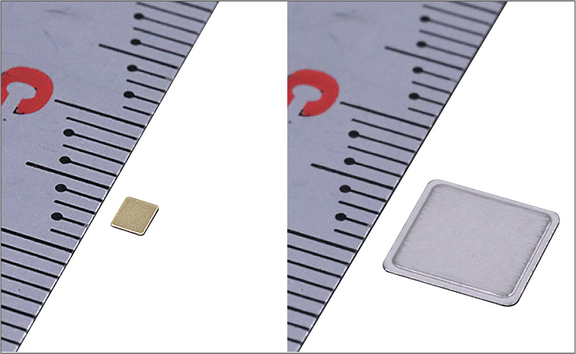
In addition to its advanced lid-manufacturing technology and expertise, YHPC boasts an impressive mass production track record when it comes to lids for crystal devices, SAW filters, and optical devices. In order to meet the stringent demands of global corporations both in Japan and abroad, we are striving to refine ourselves both in terms of people (engineers and staffers) and facilities (machinery, equipment, and lines).
 Facilities and expertise for
mass production and ultrasmall
products
Facilities and expertise for
mass production and ultrasmall
products Highly adhesive metalplating
that does not peel
even when bent 180°
Highly adhesive metalplating
that does not peel
even when bent 180° Our lines focus only on
Kovar.
Our lines focus only on
Kovar. Fully equipped with
cleanrooms for thorough
elimination of contaminants
Fully equipped with
cleanrooms for thorough
elimination of contaminants Our integrated system covers
everything from pressmachining
to metal-plating.
Our integrated system covers
everything from pressmachining
to metal-plating. Our integrated system covers
everything from pressmachining
to metal-plating.
Our integrated system covers
everything from pressmachining
to metal-plating. World leader with monthly
production of 600 million
units*³
World leader with monthly
production of 600 million
units*³ of our transactions are with
international clients.
of our transactions are with
international clients. Prototype delivery times
are extremely fast!
Prototype delivery times
are extremely fast!| Flat lids | Stepped lids | Other |
|---|---|---|
 |
 |
 |
 |
 |
 |
|
|
|
| Normal | Burr-less light cutting | Burr-less heavy cutting |
|---|---|---|
| 5~15μm | 0~3μm | 0μm |
|
|
|

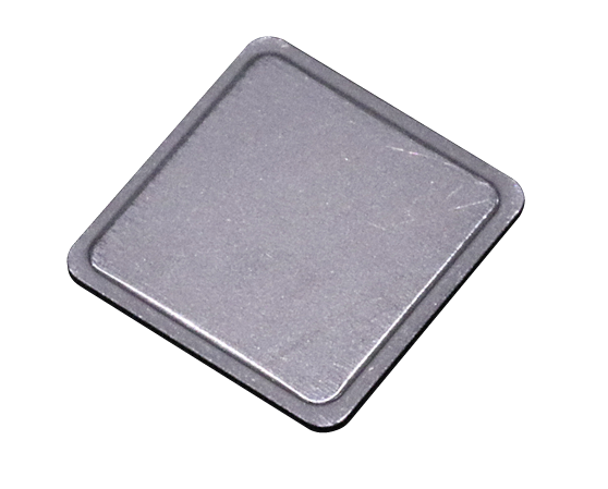
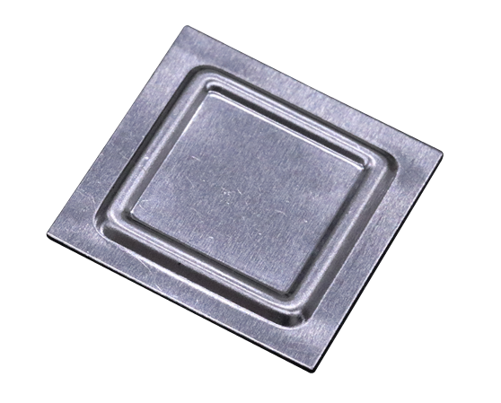
We have combined our drawing technologies to increase internal volume and lower costs.
Six keywords about cap production and
our thorough corner radius minimization
When it comes to caps for crystal devices, SAW filters, and optical devices, our press drawing technology can also provide new added value for our customers’ precision drawn products and ceramic package products.
 Package cost is reduced by
replacing lamination with
monolayers.
Package cost is reduced by
replacing lamination with
monolayers. Ultra-compact design is
achieved by putting cavities
on the metal side.
Ultra-compact design is
achieved by putting cavities
on the metal side. Internal radii are minimized
with drawn shapes.
Internal radii are minimized
with drawn shapes. Bonding areas can be secured
while maintaining
compactness.
Bonding areas can be secured
while maintaining
compactness. Flangeless caps provide
larger welding surfaces.
Flangeless caps provide
larger welding surfaces. Support for Ni and
Au metal-plating
Support for Ni and
Au metal-plating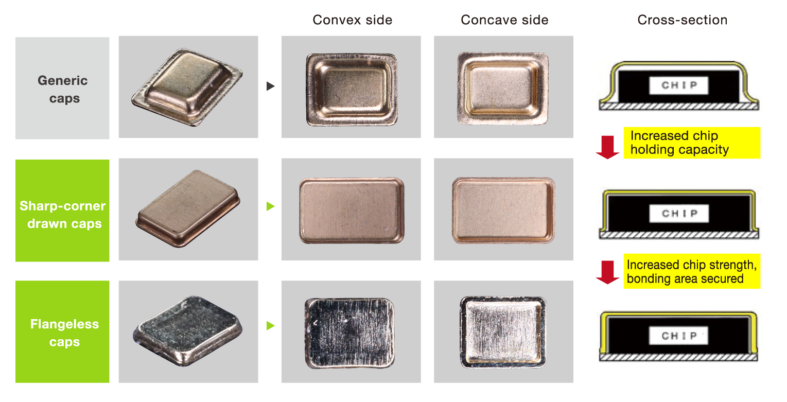
The drawing technology and expertise cultivated since our founding have enabled us to increase internal volume, achieve cap strength and rigidity, and secure bonding surface area. The IC chips and other devices that are encapsulated by our caps can be safely sealed.
